- Flex PCB Blog
- Reflow Soldering PCB Temperature Curve Explanation
- What is FPC
- Special attention points for flexible circuit wiring
- Multilayer PCB Stack-up Basics | PCB Knowledge
- PCB Protection: Potting or Conformal Coating? | PCB Knowledge
- FPCway: Specialized manufacturer of flexible printed circuit boards and rigid-flexible printed circuits
- Future Trends of Flexible Circuit Boards
- Rigid-Flex PCB Stack-up for Impedance Controlled Designs
- Control Impedance Between Rigid PCB and Flex PCB
- Flex PCB Reliability and Bendability
- Normal Flex PCB Specifications
- Flex PCB Polyimide Coverlay and Solder Mask
- Flex PCB Boards and Connectors
- About RA Copper and ED Copper
- Introduction of Flexible PCB
- 5 Tips For Designing Flexible PCB
- Advantages of FPC (Flexible PCB)
- Evolution of the Flex Printed Circuit Board
- Benefits of Using Flex Circuit Boards
- Why Rigid-Flex PCBs are Economical?
- Flexible PCB vs Rigid PCB
- Development of Flexible printed circuit board (FPC) market
- Traditional Manufacture Engineering of FPC Substrate
- Development Trend of FPC Board
- Flex PCB and the Manufacturing
- About Flex PCB design
- About Flex PCB and Assembly
- How to Ensure Flex PCB Design Success
- How to Select the Appropriate FPC Materials?
- The Differences In Rigid PCB, Flex PCB and Rigid-Flex PCB
- Flex-Rigid PCB Design Guidelines
- Beneficials for Polyimide Flex PCB Boards
- About Stiffener on Flex PCB FPC circuit Boards
- About ENIG and ENEPIG
- PCB Surface Finish Comparison
- Copper Thickness for FPC Boards
- Interconnect Solutions for Flexible Printed Circuits and Etched Foil Heaters
- Advantages and Disadvantages of Rigid-Flex PCB
- About FPC Plating Process
- About EMI shield design for Flex Printed Circuit Board
- PCB Assembly Blog
- FPC Research Blog
Special attention points for flexible circuit wiring
Layer stacking design, device layout, and cutting issues are all obvious, but there are many material weaknesses that can be encountered in flexible circuits.
From relatively high z-axis expansion coefficient adhesives to low viscosity PI substrate copper clad, to copper hardening and fatigue. The following statements of what to do and what not to do will focus on supplementing:
Maintaining the flexibility of the flexible board
It is obvious that the flexibility of the flexible circuit should be determined according to the needs in advance, but it still needs to be emphasized again. If the flexible circuit section is only intended to be folded during assembly and then installed in a fixed position, such as in a handheld ultrasound device, then we have a lot of freedom in choosing the number of layers and the type of copper skin (RA or ED). On the other hand, if the flexible circuit section is to be constantly moved, bent, or rotated, then the number of layers should be reduced and adhesive-free materials should be selected.
We can use IPC-2223B formulas (Formula 1 represents single-sided, Formula 2 represents double-sided, etc.) to determine the minimum allowable bending radius based on the allowable deformation of copper and other material properties.
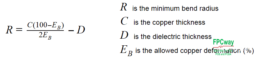
This example formula is for a single-sided flexible board.
We choose EB based on actual usage conditions, with 16% for applications with little bending, 10% for flexible mounting applications, and 0.3% for dynamic flexible designs.
Do not bend at corners
Generally, we recommend keeping the copper trace of the flexible circuit bent along the vertical direction. But sometimes it's not possible, so try to minimize the bending amplitude and frequency, or use tapered bending according to mechanical design requirements.
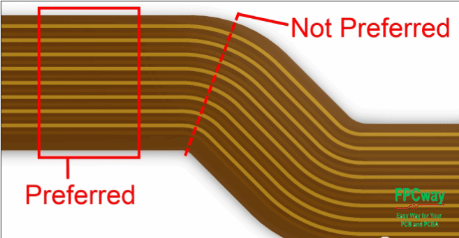
Figure 1: Preferred bending location
Use arc routing
As shown in Figure 1 above, it is best to avoid using abrupt right angles or rigidly straight 45° angle traces, but rather to use an arc angle routing pattern. This can reduce the stress on the copper during bending.
Do not suddenly change the width of the trace
When the trace is connected to the pad, especially when arranging and arranging the flexible circuit terminals (as shown in the figure below), a weak force point will be formed, and the copper skin will easily age over time. Unless a reinforcing plate is used or the application process will not bend, it is recommended to use a gradually narrowing connection method such as the one shown below.
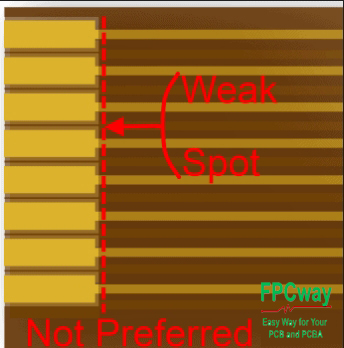
Figure 2: Sudden changes in trace width or connections to pads can create weak focal points
Use polygons
it is necessary to place a power supply or ground plane on a flexible board. If you don't mind significantly reducing flexibility and potentially causing the copper skin to wrinkle, you can choose to use solid copper. Generally speaking, it is best to use shadow polygon copper plating to maintain a high degree of flexibility. In mentioning this, I also think that traditional shadow polygons will have excess copper reinforcement in the directions of 0°, 90°, and 45°. A more optimized pattern is the hexagonal approach. This problem can be solved by using negative layer and arrayed hexagonal pads, and the shadow polygon can be established more quickly using copy and paste methods.
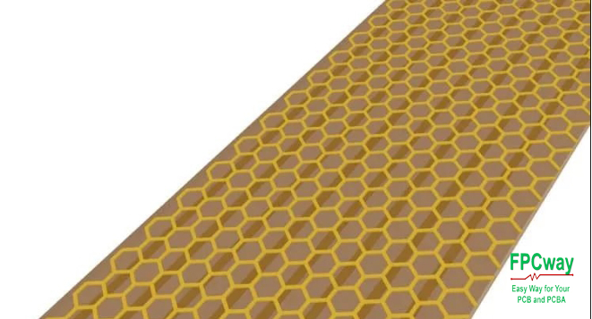
Figure 3: Using hexagonal copper plating can evenly balance the stress in three angles.
Provide reinforcement for pads
Due to the use of low-viscosity adhesives (relative to FR-4), copper on flexible circuits is more likely to detach from the polyimide substrate. Therefore, providing reinforcement for exposed copper is particularly important. Coated through holes provide appropriate anchoring for two flexible layers, so using vias is a very good reinforcement method. Because of this (providing z-axis expansion), many processing plants recommend adding coated through holes with depths up to 1.5 mils to rigid-flex boards and flexible circuits. Surface mount pads and non-coated through hole pads do not have reinforcement measures themselves, so additional reinforcement is needed to prevent detachment.
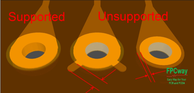
Figure 4: Reinforcement methods for flexible circuit pads, plating, increasing anchors, and reducing cover film openings
Referring to Figure 4, the second option is suitable for adhesive-type cover layers, and the third option is suitable for non-adhesive-type cover layers. Protective films using adhesives may exhibit "overflow" phenomena, so the gap between the pad and the opening must be large enough to ensure excellent soldering formation.
SMT component pads are the most fragile, especially when flexible circuits bend under the rigid pins and pads of the component. Figures 5 and 6 show how to reinforce the pads on both ends of the pad using a cover layer. To achieve this, the pads on the flexible board must be larger than the pads on a typical rigid board.
Looking at the comparison in Figure 6, SMD pads for installing components on a flexible board. This significantly reduces the installation density of flexible circuit components, but compared to rigid circuits, the density of flexible circuits cannot be too high in the first place.

Figure 5: SOW package cover film opening, showing its reinforcement on both ends of each pad. Figure 6: Adjusting pad size and cover layer openings
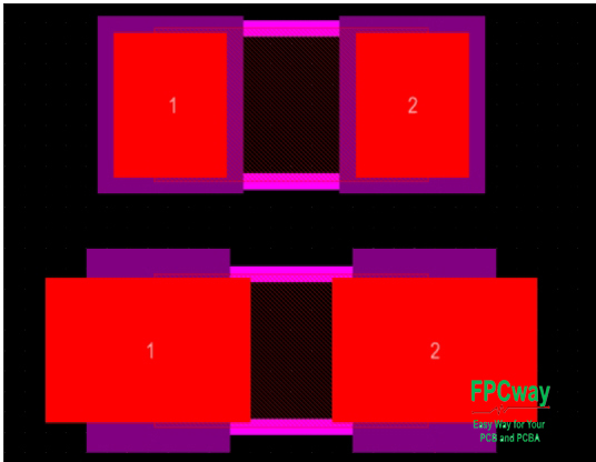
Figure 6: Adjusting pad size and cover layer openings.
Maintain double-sided flexibility
For dynamic double-sided flexible circuits, try to avoid placing traces in the same direction, but instead need to stagger them (Figure 7) to evenly distribute the copper trace (Figure 8).
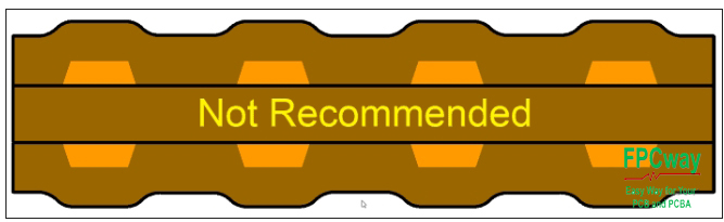
Figure 7: Not recommended adjacent layer copper trace routing.
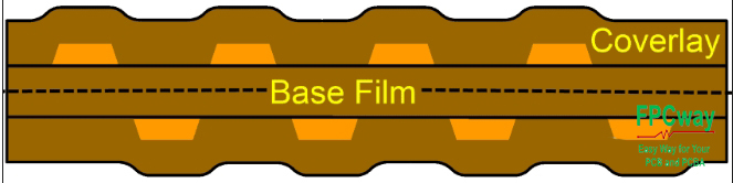
Figure 8: Preferred staggered adjacent layer copper trace routing.


