- Flex PCB Blog
- PCB Assembly Blog
- FPC Research Blog
- Preparation of FPC based on ultrasonic spraying method_4_Experimental Results
- Preparation of FPC based on ultrasonic spraying method_3_Experimental Procedure
- Preparation of FPC based on ultrasonic spraying method_2_Experimental Platform and Principle
- Preparation of FPC based on ultrasonic spraying method_1_abstract
- Research on Layout Design Method of Ultra-thin FPC_4_Analysis of Layout Design Methods
- Research on Layout Design Method of Ultra-thin FPC_3_Analysis of Layout Design Methods
- Research on Layout Design Method of Ultra-thin FPC_2_Analysis of Layout Design Methods
- Research on Layout Design Method of Ultra-thin FPC_1_introduction
- Research progress on polyimide FPC_2_the field of FPC
- Research progress on polyimide FPC_1_Introduction
- Analysis of Vibration Characteristics of FPCBs _4_Summary
- Analysis of Vibration Characteristics of FPCBs _3_Finite Element Analysis
- Analysis of Vibration Characteristics of FPCBs _2_Theory of Vibration Analysis
- Analysis of Vibration Characteristics of FPCBs Under Random Vibration_1_Introduction
- Design Methods for FPCBs_5_Practical Application
- Design Methods for FPCBs_4_Electrical Circuit Design and Examples
- Design Methods for FPCBs_3_Structure Design Method and Examples
- Design Methods for FPCBs_2_Component Selection Methodology and Examples.
- Research on Design Methods for FPCBs
- Application of MPW technique for FPCBs _4_Summary
- Application of MPW technique for FPCBs_3_Experimental results
- Application of MPW technique for FPCBs_2_Experimental setup
- Application of MPW technique for FPCBs_1_Principle of MPW
- Application of FPCB in PC motherboards_4_ Results and discussion
- Application of FPCB in PC motherboards_3_ Numerical analysis
- Application of FPCB in PC_2_ Experimentation
- Application of FPCB in PC motherboards
- A Bus Planning Algorithm for FPC Design _4_Experimental result
- A Bus Planning Algorithm for FPC Design _3_Proposed Algorithm
- A Bus Planning Algorithm for FPC Design _2_Preliminaries
- A Bus Planning Algorithm for FPC Design _1_Introduction
Preparation of FPC based on ultrasonic spraying method_4_Experimental Results
3. Experimental Results
3.1 Conductivity Testing and Analysis
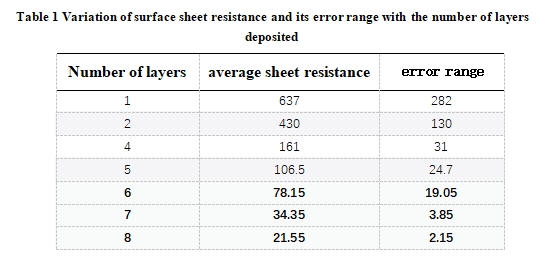
The conductivity of the circuit was judged by measuring the sheet resistance of the conductive lines with different numbers of spray layers. To ensure the accuracy and authenticity of the experimental data, five random points were selected for testing on each individual sample, and then the average value and error range were calculated. Table 1 shows the impact of different numbers of spray layers (each layer sprayed under the conditions of a solution feed rate of 0.15 mL/min and a nozzle movement speed of 20 mm/s) on the circuit sheet resistance. As the number of spray layers increases, the sheet resistance steadily decreases, and the corresponding error also narrows. In actual industrial production, it is generally considered that a sheet resistance of less than 100 mΩ/sq is already a very good conductive effect. Therefore, under the experimental conditions of this study, excellent conductivity can be achieved when the number of spray layers reaches 6 or more.
3.2 Macroscopic Morphology and Edge Roughness
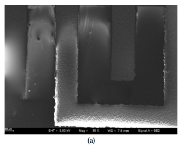
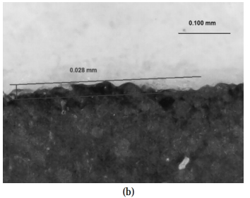
Based on the results of the conductivity tests, circuits with 6 to 8 spray layers were selected for subsequent related tests. The edge morphology of the 8-layer sprayed circuit was observed under a microscope. Figure 6a shows the morphological characteristics of the circuit at a magnification of 30 times, with the corners clearly demonstrated; a randomly cropped image of a portion of the rough edge (see Figure 6b) was used to calculate the corresponding roughness proportionally. It was found that the edge roughness error could be controlled within 0.05 mm (50 μm), indicating that the resulting lines are smooth and flat.
3.3 XRD and SEM Characterization
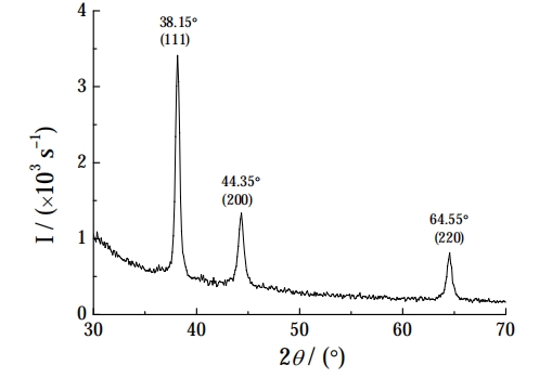
Figure 7 shows the X-ray diffraction spectrum of a 6-layer sprayed sample. Obvious peaks are observed near 38°, 44°, and 64°, which correspond exactly to the diffraction angles of silver. Due to the presence of the substrate PI film's diffraction, there is some background noise, but it is sufficient to prove that the wires on the substrate are composed of pure silver.
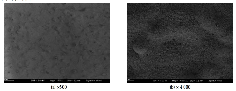
By observing the microstructure of the silver wire surface through SEM, the results are shown in Figure 8. It can be seen that the microstructure of the lines is uniform and flat, which verifies the high precision characteristics of the ultrasonic spraying method.
