- Flex PCB Blog
- PCB Assembly Blog
- FPC Research Blog
- Preparation of FPC based on ultrasonic spraying method_4_Experimental Results
- Preparation of FPC based on ultrasonic spraying method_3_Experimental Procedure
- Preparation of FPC based on ultrasonic spraying method_2_Experimental Platform and Principle
- Preparation of FPC based on ultrasonic spraying method_1_abstract
- Research on Layout Design Method of Ultra-thin FPC_4_Analysis of Layout Design Methods
- Research on Layout Design Method of Ultra-thin FPC_3_Analysis of Layout Design Methods
- Research on Layout Design Method of Ultra-thin FPC_2_Analysis of Layout Design Methods
- Research on Layout Design Method of Ultra-thin FPC_1_introduction
- Research progress on polyimide FPC_2_the field of FPC
- Research progress on polyimide FPC_1_Introduction
- Analysis of Vibration Characteristics of FPCBs _4_Summary
- Analysis of Vibration Characteristics of FPCBs _3_Finite Element Analysis
- Analysis of Vibration Characteristics of FPCBs _2_Theory of Vibration Analysis
- Analysis of Vibration Characteristics of FPCBs Under Random Vibration_1_Introduction
- Design Methods for FPCBs_5_Practical Application
- Design Methods for FPCBs_4_Electrical Circuit Design and Examples
- Design Methods for FPCBs_3_Structure Design Method and Examples
- Design Methods for FPCBs_2_Component Selection Methodology and Examples.
- Research on Design Methods for FPCBs
- Application of MPW technique for FPCBs _4_Summary
- Application of MPW technique for FPCBs_3_Experimental results
- Application of MPW technique for FPCBs_2_Experimental setup
- Application of MPW technique for FPCBs_1_Principle of MPW
- Application of FPCB in PC motherboards_4_ Results and discussion
- Application of FPCB in PC motherboards_3_ Numerical analysis
- Application of FPCB in PC_2_ Experimentation
- Application of FPCB in PC motherboards
- A Bus Planning Algorithm for FPC Design _4_Experimental result
- A Bus Planning Algorithm for FPC Design _3_Proposed Algorithm
- A Bus Planning Algorithm for FPC Design _2_Preliminaries
- A Bus Planning Algorithm for FPC Design _1_Introduction
Research on Layout Design Method of Ultra-thin FPC_2_Analysis of Layout Design Methods
This article focuses on two main aspects of ultra-thin FPC analysis: (1) Research and analysis of trace parasitic capacitances. This aspect aims to ensure the signal integrity of the traces by using a commonly used (glass fiber epoxy resin copper clad laminate FR-4) printed circuit board as a benchmark. Through design, the parasitic capacitances of ultra-thin FPC traces are made close to those of FR-4, thereby ensuring the signal integrity of the FPC. (2) Analysis of EMC shielding isolation for mesh reference planes. This aspect aims to achieve better EMC shielding effectiveness by analyzing and researching the mesh size, mesh ratio, and mesh pattern of the mesh reference plane, and proposing better design methods.
1.1 Solid Copper Reference Plane Analysis
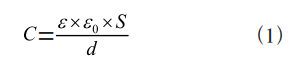
The solid copper reference plane, due to its complete flatness, possesses excellent EMC shielding performance. However, as the layer spacing in ultra-thin FPCs decreases, the parasitic capacitances between traces inevitably increase, which affects the edge rate of the transmitted signals, reduces the transmission bandwidth, and leads to significant signal integrity issues. The calculation of parasitic capacitances is illustrated in Figure 1.
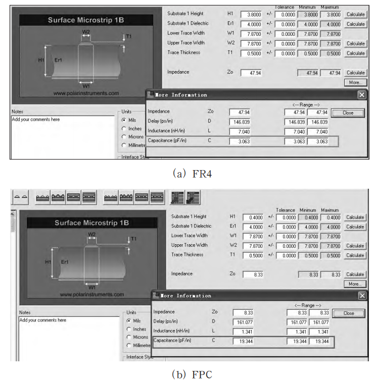
Figure 1(a) shows the parasitic capacitance C for a solid copper reference plane FR4 trace (with a layer spacing of 3.8 mil and a trace width of 8 mil), which is approximately 3 pF/Inch. Figure 1(b) presents the parasitic capacitance C for an FPC trace on a solid copper reference plane (with a layer spacing of 0.4 mil and a trace width of 8 mil), which is about 19 pF/Inch.
Typically, the length of FPC cables used in products reaches about 8 inches, which would generate a parasitic capacitance of 150 pF. This level of parasitic capacitance causes severe transmission losses and may even prevent signals from being transmitted normally.
To address the aforementioned issue, the following text will explore changing the trace width to reduce parasitic capacitances.
Calculating the parasitic capacitance of traces using the capacitor formula:
Normal FR4 trace capacitance C (solid copper reference plane, with d greater than 3.8 mil, and a trace width between 3.5 and 8 mil);
The parasitic capacitance C' of FPC traces on a solid copper reference plane is calculated as follows: S represents the projection area of the trace on the reference plane, d is the layer spacing, ε and ε0 are the dielectric constants. The projection area S is equal to the product of the trace width W and the trace length L.

S′ is the projection area of the trace on the reference plane, which is numerically equal to the projection area S of the FR4 trace when using a solid copper reference plane. d′ represents the layer spacing of the FPC.
The design goal is to make the trace capacitance of the solid copper reference plane FPC close to that of a normal FR4 trace, that is, to achieve C′ /C = 1.
When the trace length L is fixed, the width ratio of the FPC trace to the normal FR4 trace must satisfy W′ /W = d′ /d. The normal width W ranges from 3.5 to 8 mils, and the ratio d′ / d is generally around 4 to 8 mils. Therefore, W′ needs to be less than 2 mils. However, current PCB manufacturing processes cannot achieve such a narrow linewidth, and it would also have very low reliability, with a high risk of breaking during bending.
Consequently, among the three design methods for ultra-thin FPCs, the solid copper reference plane design is no longer applicable. To design an ultra-thin FPC that can transmit high-speed signals and has good EMC performance, one must use a mesh copper reference plane design.


