- Flex PCB Blog
- PCB Assembly Blog
- How to solve the problem of PCB warping deformation after welding large copper bar?
- About PCB Assembly
- QFP and BGA and the Development Trend in PCB assembly
- Why some components need be baked before reflow soldering
- About Flex PCB Assembly
- Manual Soldering in SMT Assembly Manufacturing Process
- BGA Components and BGA Assembly
- Quick Understanding for PCB Assembly Process
- About SMT Assembly (Surface Mount Technology)
- About THT Assembly (Through-Hole Technology)
- About Reflow Soldering
- About_Wave_Soldering
- PCB Assembly Inspections and Tests
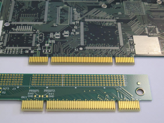
- Panel Requirements for PCB Assembly
- About SMT (Surface Mount Technology)
- FPC Research Blog
Through-hole technology (THT) that started flourishing with IC (integrated circuit) in 60s has been gradually replaced by the first generation of SMT (surface mount technology) that came onto the stage as early as 80s along with the rapid development of LSI at the later phase of 70s. Peripheral packages have become the main stream of electronics packages with QFP (quad flat package) as an example. 90s has witnessed fine pitch of QFP, leading board assembly technology to meet lots of challenges. In spite of the advent of fine pitch technology (FPT), board-level circuit assembly with pitch lower than 0.4mm still features many technical issues that should be dealt with. As an optimal solution, the second generation of SMT was released at the former phase of 90s, that is, BGA (ball grid array) package. Then, chip-scale package (CSP) became people's focus in 1990s. Especially when flip chip (FC) technology is used, PBGA (plastic ball grid array) starts to be applied in super computers and work stations and gradually become practical. The third generation of SMT is direct chip assembly (DCA) that is only applied in special fields due to limitations in terms of reliability, cost and KGD etc. Recent years has seen the participation of wafer level packaging (WLP) and advanced FC in the third generation of SMT compatible with the requirement of semiconductor multiple pins and high performance. Therefore, it can be concluded that IC packages in the 21st century will develop towards trends of high density, fine pitch, high flexibility, high reliability and diversity. As a result, it's of much significance to be aware of the difference between QFP and BGA and their development trend.
Plastic Quad Flat Package (PQFP)
PQFP obviously features competitive advantages in IC packaging market. Nowadays, electronics package is moving towards packages BGA, CSP and ultra-fine pitch QFP due to their high added value. With pin count constantly rising, if pin count is higher than 200 with pin spacing lower than 0.5mm, pin spacing is approximately 0.3mm as far as packages with 300 pins are concerned. The smaller pin spacing is, product loss will exponentially go up. As pin spacing becomes smaller, bridging soldering will more easily take place. If pin spacing is 0.3mm, even a few particles with diameters less than 15μm will bring forward solder balling, which is a usual cause of bridging. It's even more significant to control solder paste particle size. Once pin spacing becomes smaller, it's essential to control lead planarity and spacing tolerance. When it comes to QFP, a size (40mm2), pin count (360) and pitch (0.3mm) have arrived at a limitation. Obviously, QFP is so easy to be tested and reworked that all the leads on QFP can be seen.
BGA
• Comparison between BGA and QFP
Typical BGA components are so durable that they can still be used for assembly even if they accidentally fall onto the floor, which is impossible for PQFP to some extent. The essential advantage of BGA packages lies in its array form and generally speaking BGA components are capable of providing more I/O within the same unit area than QFP components. Whenever I/O count exceeds 250, the space accounted by BGAs is always smaller than QFPs. Since BGA usually features larger pitch than QFP, BGA components are more easily mounted so that relatively high efficiency will be generated. When defects concerned with packaging are tested prior to assembly, assembly failure rate can be lower than 1ppm. Up to now, the biggest challenge confronted by BGA assembly lies in defect issues associated with packages that probably derive from missing solder balls, humidity sensitivity, collision during shipping process and excessive warpage during reflow soldering. A huge deviation is available in terms of solder ball size, which is twice or three times of volume deviation between solder balls. Double-layer solder balls possibly exist at the position of solder joint and defects related with metallization such as insufficient soldering between solder balls and component pad. Due to technique, BGA assembly allows for the lowest defect rate (ppm).
The construction of BGA packages features shorter leads than QFP with equivalent functions and performance, which leads to excellent electrical performance of BGA packages. However, the largest defect of BGA construction lies in its cost. BGA features higher cost than QFP in terms of laminate board and resin cost correlated with substrate carrying components. BT resin, ceramic and polyimide resin carrier contains original components with higher cost while QFP contains plastic molding resin and metal sheet lead frame with low cost. Array carrier features quite large cost due to fine line circuits and chemical processing technology. Furthermore, with QFP and BGA packages compared, high-output forming die and molding press equipment can be applied with fewer packaging technical procedures. Once volume production is applied, BGA package cost will be reduced but it isn't possible for it to fall to the extent of QFP.
As far as BGA package cost is concerned, BGA package with suitable number of I/O pins will be the most prevalent. This type of package contains all the circuits at the side of package carrier and carries no regulated through holes. Thus, extra cost has to be held by BGA package. However, the extremely high assembly efficiency of BGA packages can locally compensate for their disadvantage of high cost. From the perspective of economic value, when I/O pins are fewer than 200, QFP works suitably. When I/O pins exceeds 200, QFP doesn't work and multiple types of BGA packages can be applied, leading to the wide range of applications of BGA packages.
• Inspection and Rework of BGA Packages
BGA inspection and rework is also a type of technology that gradually comes into maturity. Although it can be inspected, BGA calls for high-precision equipment such as X-ray imaging system.
BGA components hide their connections under packages, leading to more difficulties of rework than components with leads at periphery. Leading issues concerning BGA rework include: damage on detachable parts, damage on replacement parts, over heating of board and adjacent components, board warpage due to local heating and cleaning and manufacturing of some parts. Rework has to take the following issues into consideration: chip temperature, temperature distribution of components within rework period and board temperature distribution. If all the necessary devices need purchasing, BGA rework station will be costly for the following reasons:
a. It's impossible to modify only one short circuit or open circuit defect and rework has to be carried out on all assembly defects of BGA.
b. Rework is more difficultly implemented than QFP, calling for added equipment investment.
c. BGA components after rework can be no longer used while QFP components can. Therefore, mass production of BGA packages derives from assembly defect reduction, ensuring high pass rate.
• Cleaning of BGA Packages
The protruding disadvantage of BGA packages lies in their incapability to clean off flux left at the bottom of array packages. Up to now, the size of BGA components with high number of pins is approximately 45mm2. Therefore, cleaning issue becomes so significant. BGA cleaning requires that all flux and solder paste has to be cleaned off because they could possibly lead to electrical failure or signal leakage to the ground in high-power applications.
Development Trend in PCB Assembly
It can be forseen that PQFP with lead number lower than 200 will be the primary packaging technology. As lead number exceeds 350, it's impossible for QFP to be widely applied. Two types of packaging technologies are available as competitors for components with I/O pins from 200 to 300. Therefore, QFP packaging technology with pitch less than 0.5mm will be definitely replaced by BGA packages.
For PCB and PCB Assembly, you can always trust us and we always able to meet your requirements and provide you the best quality boards. Feel free to contact us know for your EMS project.


