- Flex PCB Blog
- Reflow Soldering PCB Temperature Curve Explanation
- What is FPC
- Special attention points for flexible circuit wiring
- Multilayer PCB Stack-up Basics | PCB Knowledge
- PCB Protection: Potting or Conformal Coating? | PCB Knowledge
- FPCway: Specialized manufacturer of flexible printed circuit boards and rigid-flexible printed circuits
- Future Trends of Flexible Circuit Boards
- Rigid-Flex PCB Stack-up for Impedance Controlled Designs
- Control Impedance Between Rigid PCB and Flex PCB
- Flex PCB Reliability and Bendability
- Normal Flex PCB Specifications
- Flex PCB Polyimide Coverlay and Solder Mask
- Flex PCB Boards and Connectors
- About RA Copper and ED Copper
- Introduction of Flexible PCB
- 5 Tips For Designing Flexible PCB
- Advantages of FPC (Flexible PCB)
- Evolution of the Flex Printed Circuit Board
- Benefits of Using Flex Circuit Boards
- Why Rigid-Flex PCBs are Economical?
- Flexible PCB vs Rigid PCB
- Development of Flexible printed circuit board (FPC) market
- Traditional Manufacture Engineering of FPC Substrate
- Development Trend of FPC Board
- Flex PCB and the Manufacturing
- About Flex PCB design
- About Flex PCB and Assembly
- How to Ensure Flex PCB Design Success
- How to Select the Appropriate FPC Materials?
- The Differences In Rigid PCB, Flex PCB and Rigid-Flex PCB
- Flex-Rigid PCB Design Guidelines
- Beneficials for Polyimide Flex PCB Boards
- About Stiffener on Flex PCB FPC circuit Boards
- About ENIG and ENEPIG
- PCB Surface Finish Comparison
- Copper Thickness for FPC Boards
- Interconnect Solutions for Flexible Printed Circuits and Etched Foil Heaters
- Advantages and Disadvantages of Rigid-Flex PCB
- About FPC Plating Process
- About EMI shield design for Flex Printed Circuit Board
- PCB Assembly Blog
- FPC Research Blog
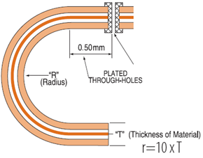 |  |
The most frequently asked question we receive regarding flex circuits is “how much can I bend a flex?”
The standard IPC answer is 10 times the thickness of the material. There is a section in IPC-2223 that offers reasonable information on bend radius calculations. But there are other factors that need consider when designing a flex circuit for high reliability.
1. Grain direction in the copper is important for tight bend radii.
2. The stiffness of a flex is primarily driven by the copper weight but kapton thickness is also critical.
3. Where is the bend located?
Here are some other thoughts of how to increase reliability for a flex circuit application.
REDUCE OVERALL THICKNESS IN THE FLEX AREA
1. Reduce the base copper weight (and the corresponding adhesive thicknesses) or reduce the dielectric thickness.
2. Use adhesiveless base materials. Adhesiveless materials will usually reduce the starting thickness of each substrate by 12-25um (0.0005”- 0.0010”) when compared to adhesive based substrates.
3. Eliminate copper plating on the conductors in the flexing area (dynamic region) by utilizing selective (pads plating/button plating-only) allowing the circuit to have increased flexibility.
MAKE THE CIRCUIT ROBUST TO WITHSTAND FLEXING
1. Conductors should be staggered from layer to layer and not stacked on top of each other to increase flexibility.
2. Conductor thickness and width should remain constant in bending areas.
3. Balance the conductor weights and material thicknesses on each side of the neutral bend axis.
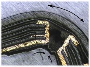
4. Bend radius of a flex should be approximately 10 times the material thickness and at least 500um (0.020”) away from the plated through hole.
5. Incorporate tear stops or reliefs for slits in the circuit. The end of the slit represents a vulnerable point for a tear to start and to propagate.


