- Flex PCB Blog
- PCB Assembly Blog
- FPC Research Blog
- Preparation of FPC based on ultrasonic spraying method_4_Experimental Results
- Preparation of FPC based on ultrasonic spraying method_3_Experimental Procedure
- Preparation of FPC based on ultrasonic spraying method_2_Experimental Platform and Principle
- Preparation of FPC based on ultrasonic spraying method_1_abstract
- Research on Layout Design Method of Ultra-thin FPC_4_Analysis of Layout Design Methods
- Research on Layout Design Method of Ultra-thin FPC_3_Analysis of Layout Design Methods
- Research on Layout Design Method of Ultra-thin FPC_2_Analysis of Layout Design Methods
- Research on Layout Design Method of Ultra-thin FPC_1_introduction
- Research progress on polyimide FPC_2_the field of FPC
- Research progress on polyimide FPC_1_Introduction
- Analysis of Vibration Characteristics of FPCBs _4_Summary
- Analysis of Vibration Characteristics of FPCBs _3_Finite Element Analysis
- Analysis of Vibration Characteristics of FPCBs _2_Theory of Vibration Analysis
- Analysis of Vibration Characteristics of FPCBs Under Random Vibration_1_Introduction
- Design Methods for FPCBs_5_Practical Application
- Design Methods for FPCBs_4_Electrical Circuit Design and Examples
- Design Methods for FPCBs_3_Structure Design Method and Examples
- Design Methods for FPCBs_2_Component Selection Methodology and Examples.
- Research on Design Methods for FPCBs
- Application of MPW technique for FPCBs _4_Summary
- Application of MPW technique for FPCBs_3_Experimental results
- Application of MPW technique for FPCBs_2_Experimental setup
- Application of MPW technique for FPCBs_1_Principle of MPW
- Application of FPCB in PC motherboards_4_ Results and discussion
- Application of FPCB in PC motherboards_3_ Numerical analysis
- Application of FPCB in PC_2_ Experimentation
- Application of FPCB in PC motherboards
- A Bus Planning Algorithm for FPC Design _4_Experimental result
- A Bus Planning Algorithm for FPC Design _3_Proposed Algorithm
- A Bus Planning Algorithm for FPC Design _2_Preliminaries
- A Bus Planning Algorithm for FPC Design _1_Introduction
Design Methods for FPCBs_4_Electrical Circuit Design and Examples
Before conducting flexible printed circuit board electrical circuit design, it is necessary to first clarify the product wiring table. The following questions need to be addressed:
1.What signals are in the product? Based on the point signal definition in the wiring table or communication with the user, confirm the type of point signal that the product needs to handle.
2. What are the requirements for signals in the product? Based on the point signal requirements in the wiring table or communication with the user, confirm the specific requirements for the point signals that the product needs to handle, such as whether differential signaling is required, impedance matching, signal overcurrent size, and power supply signal voltage drop requirements.
3. Definition of circuit design rules. After clarifying the signal types and requirements in steps 1 and 2, we can confirm the wiring width, line spacing, and copper thickness of signals according to QJ3103-99 "Printed Circuit Board Design Specification". Considering the derating level, we can start electrical circuit design based on customized design rules.
4. Stacked layer design of flexible printed circuit boards. Since flexible printed circuit boards are designed with irregular routing structures based on equipment system space structures, it is also necessary to determine its stacked layer structure based on the three-dimensional structural layout of the flexible printed board to ensure that the produced flexible printed circuit board can meet the assembly requirements of actual products.
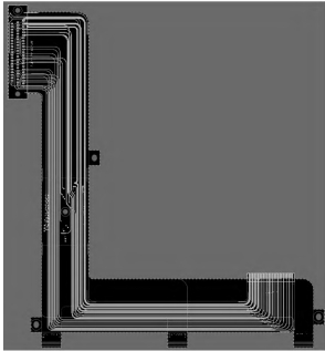
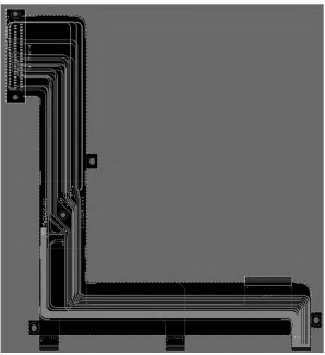
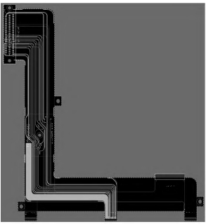
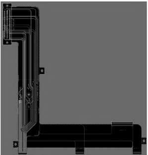
Taking the electrical circuit design of a 5-terminal flexible printed circuit board as an example, the product connections mainly include power signals, ordinary analog signals, and ground signals. The overcurrent requirement for ordinary analog signals is 0.2A; the power signal requires an overcurrent of 1.3A, with the smaller the conduction voltage drop being better; the ground signal is connected to the shell ground. The product routing design is based on QJ3103-99 and the flexible board structural dimensions, confirming that the ordinary analog signal line width is 10mil, the power signal line width is 80mil, and the copper thickness is 1Oz. After calculation, the minimum power supply voltage drop is 0.3Ω. Due to the sorting of the routing structure, a stacked layer design was also performed for the flexible printed board, which consists of the J30J straddle surface mount component layer, J63A(1) straddle surface mount component layer, J63A(2) straddle surface mount component layer, and J63A(3) straddle surface mount component layer from top to bottom. The electrical circuit design of the 5-terminal flexible printed circuit board is shown in the figure.

Figure 5 Signal Layer 1 /2

Figure 6 Signal Layer 3 /4

Figure 7 Signal Layer 5 /6

Figure 8 Signal Layer 7/8


