- Flex PCB Blog
- PCB Assembly Blog
- How to solve the problem of PCB warping deformation after welding large copper bar?
- About PCB Assembly
- QFP and BGA and the Development Trend in PCB assembly
- Why some components need be baked before reflow soldering
- About Flex PCB Assembly
- Manual Soldering in SMT Assembly Manufacturing Process
- BGA Components and BGA Assembly
- Quick Understanding for PCB Assembly Process
- About SMT Assembly (Surface Mount Technology)
- About THT Assembly (Through-Hole Technology)
- About Reflow Soldering
- About_Wave_Soldering
- PCB Assembly Inspections and Tests
- Panel Requirements for PCB Assembly
- About SMT (Surface Mount Technology)
- FPC Research Blog
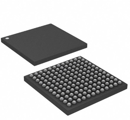
Classifications and Properties of BGA Components
• Classifications of BGA Components
Based on different packaging materials, BGA components can be classified into the following types: PBGA (plastic ball grid array), CBGA (ceramic ball grid array), CCGA (ceramic column grid array), TBGA (tape ball grid array) and CSP (chip-scale package). Here's an article giving details concerning advantages and disadvantages of those types of BGA components.
• Properties of BGA Components
The leading properties BGA components hold include:
a. I/O lead pitch is so large that more I/O count can be held within the same area.
b. Higher packaging reliability, lower defect rate of solder joints and higher reliability of solder joints.
c. Alignment of QFP (quad flat package) chips is usually achieved by visual observation carried out by operators and it's difficult for alignment and soldering. However, it's easier to implement alignment and soldering on BGA components due to relatively large pin pitch.
d. It's easier to carry out solder paste printing through stencil on BGA components.
e. BGA pins are steady with better flatness than QFP package because flatness error can be automatically compensated between chip and PCB (printed circuit board) after solder ball melting.
f. During soldering process, tension between solder joints will lead to high self-alignment that allows mounting precision error of 50%.
g. Featuring excellent electrical properties, BGA components make it possible to obtain excellent frequency merits.
h. BGA components perform better in terms of thermal dissipation.
Naturally, apart from advantages, BGA components also feature disadvantage. One leading disadvantage is that it's difficult to inspect quality of solder joints, which depends on AXI (automated X-ray inspection) and AOI (automated optical inspection) equipment that are capable of observing solder ball collapse. Of course, inspection cost and difficulty rise as well.
Storage and Application Environment of BGA Components
BGA components are a type of highly humidity and thermal-sensitive components, so they should be stored in the dry environment with constant temperature. Moreover, operators should rigorously conform to operation technology process to stop components from bad effect prior to assembly. Generally speaking, the optimal storage environment for BGA components is within the temperature range from 20°C to 25°C with humidity less than 10%RH. Furthermore, they should best be stored by nitrogen gas.
Generally, after BGA component packages are opened, they should never be exposed to the air for long time during assembly and soldering process to stop components from leading to soldering quality reduction due to their low quality. Once packages of BGA components are opened, they have to be used up within 8 hours in the operation environment of ≤30°C/60%RH. When components are stored in nitrogen, application time can be prolonged to some extent.
It's extremely common to see that BGA components fail to be used up once their packages are opened during SMT (surface mount technology) assembly. BGA components have to be baked prior to their applications next time to capture their excellent solderability. Baking temperature usually maintains at 125°C. Relationship between baking time and package thickness can be summarized in below table.
| Package Thickness (t/mm) | Baking Time (h) |
| t≤1.4 | 14 |
| 1.4<t≤4.0 | 24 |
Too high baking temperature will lead to a modification of metallographic structure at the connection between solder balls and components. Detachment tends to be generated between solder balls and component packaging with SMT assembly quality decreased. When baking temperature is too low, dehumidification will fail to be obtained. BGA components can be assembled after baking and cooling for 30 minutes in natural environment.
BGA Component Soldering Technologies
BGA component assembly technologies are fundamentally compatible with SMT. Leading soldering phases come as solder paste printing on pad array by stencil and BGA components alignment to pad array, reflow soldering of BGA components. In the rest of this article, a brief introduction will be provided on PBGA soldering process.
• Solder Paste Printing
Solder paste quality plays a key role in affecting soldering quality. The following aspects should be considered when selecting solder paste: excellent printability, excellent solderability and less contaminant.
Particle diameter of solder paste should be compatible with lead pitch of components. Generally, the smaller lead pitch is, the smaller solder paste particle diameter, the better printing quality will be. But it's never that simple as solder paste with larger particle diameter leads to higher soldering quality than that with smaller particle diameter. Therefore, comprehensive considerations should be taken when determining solder paste. Because BGA components feature fine pitch, it's suitable to select solder paste with particle diameter below 45μm to guarantee excellent printing effect and soldering effect.
Stencil used for solder paste printing is made of stainless material. Since BGA components feature fine pitch, stencil thickness should be limited within the common range from 0.12mm to 0.15mm. Stencil opening is usually determined by components and it's a common case that stencil opening is smaller than pad and is generated by laser cutting.
During printing process, a stainless metal scraper with 60 degrees is applied whose printing pressure is controlled within the range from 35N to 100N. Either too high or too low pressure is bad for printing. Printing speed is controlled within the range from 10mm/s to 25mm/s. The smaller opening pitch is, the slower printing will be. Furthermore, field temperature of operation is required to be at approximately 25°C and humidity at the range from 55% to 75%RH. PCB boards after solder paste printing should enter reflow soldering oven after 30 minutes of solder paste printing to stop solder paste from being exposed to the air for long time with product quality reduced.
• Component Mounting
The essential aim of mounting is to get each solder balls on BGA components aligned with each pad on PCB board. Because BGA component pins are too short to be easily seen by naked eyes, specialized equipment should be used for accurate alignment. Up to now, primary equipment for accurate alignment includes BGA/CSP rework station and chip mounter among which precision of chip mounter reaches approximately 0.001mm. With mirror recognition leveraged, BGA components can be accurately mounted on pad array on circuit board.
Nevertheless, BGA components fail to ensure 100% excellent solder balls through mirror recognition and some solder ball on Z axis may be smaller than other balls. To guarantee excellent solderability, BGA components can be reduced by 25.41μm to 50.8μm by height and delay shutdown vacuum system is applied for 400ms. With solder balls and solder paste totally contacted, void soldering of BGA components can be decreased.
• Reflow Soldering
Reflow soldering is the most difficult-controlled phase in BGA assembly process, so optimal reflow soldering curve achievement is a key element contributing to excellent BGA soldering. Reflow soldering curve contains four phases: preheating, soaking, reflow and cooling. Temperature and time of the four phases can be respectively set and modified so that optimal soldering result can be acquired.
• BGA Rework
BGA rework after soldering is carried out on a BGA rework station that can solder and rework independently on a BGA chip without affecting adjacent components. Therefore, a hot air reflow nozzle with suitable size can be selected to cover BGA chip for the convenience of soldering.
BGA Component Soldering Quality Inspection
BGA as a short form of ball grid array packaging contain solder balls under components and quality of solder balls can hardly be known without specific inspection devices. Visual inspection alone fails to acquire soldering quality of solder joints. Up to now, inspection devices for BGA soldering quality inspection are X-ray inspection devices that are classified into two categories: 2D and 5D.
2D X-ray inspection devices can inspect soldering issues such as cracks, missing, bridging, misalignment and insufficient solder with a low cost. Nevertheless, a primary disadvantage of 2D X-ray inspection devices is that it's sometimes a little difficult to distinguish which side a component image reflects if two images are overlapped. This advantage can be overcome when a 5D X-ray inspection device is relied, just with a higher cost.


