- Flex PCB Blog
- PCB Assembly Blog
- FPC Research Blog
- Preparation of FPC based on ultrasonic spraying method_4_Experimental Results
- Preparation of FPC based on ultrasonic spraying method_3_Experimental Procedure
- Preparation of FPC based on ultrasonic spraying method_2_Experimental Platform and Principle
- Preparation of FPC based on ultrasonic spraying method_1_abstract
- Research on Layout Design Method of Ultra-thin FPC_4_Analysis of Layout Design Methods
- Research on Layout Design Method of Ultra-thin FPC_3_Analysis of Layout Design Methods
- Research on Layout Design Method of Ultra-thin FPC_2_Analysis of Layout Design Methods
- Research on Layout Design Method of Ultra-thin FPC_1_introduction
- Research progress on polyimide FPC_2_the field of FPC
- Research progress on polyimide FPC_1_Introduction
- Analysis of Vibration Characteristics of FPCBs _4_Summary
- Analysis of Vibration Characteristics of FPCBs _3_Finite Element Analysis
- Analysis of Vibration Characteristics of FPCBs _2_Theory of Vibration Analysis
- Analysis of Vibration Characteristics of FPCBs Under Random Vibration_1_Introduction
- Design Methods for FPCBs_5_Practical Application
- Design Methods for FPCBs_4_Electrical Circuit Design and Examples
- Design Methods for FPCBs_3_Structure Design Method and Examples
- Design Methods for FPCBs_2_Component Selection Methodology and Examples.
- Research on Design Methods for FPCBs
- Application of MPW technique for FPCBs _4_Summary
- Application of MPW technique for FPCBs_3_Experimental results
- Application of MPW technique for FPCBs_2_Experimental setup
- Application of MPW technique for FPCBs_1_Principle of MPW
- Application of FPCB in PC motherboards_4_ Results and discussion
- Application of FPCB in PC motherboards_3_ Numerical analysis
- Application of FPCB in PC_2_ Experimentation
- Application of FPCB in PC motherboards
- A Bus Planning Algorithm for FPC Design _4_Experimental result
- A Bus Planning Algorithm for FPC Design _3_Proposed Algorithm
- A Bus Planning Algorithm for FPC Design _2_Preliminaries
- A Bus Planning Algorithm for FPC Design _1_Introduction
Research on Layout Design Method of Ultra-thin FPC_3_Analysis of Layout Design Methods
1.2 Mesh Copper Reference Plane Analysis
The mesh reference plane is one of the commonly used design methods, which has two advantages. Firstly, the mesh reference plane can make the finished cable more flexible. Secondly, it has a certain effect on EMC (Electromagnetic Compatibility). However, the current commonly used mesh reference plane design has some defects and tends to be more arbitrary. There is a lack of research on aspects such as mesh size, mesh ratio, and mesh form, which often leads to poor shielding effectiveness of the manufactured mesh reference plane, and even the situation where both signal integrity and EMC effects are unsatisfactory. This article mainly focuses on this aspect for research and analysis, striving to achieve optimization of mesh design. The specific analysis is as follows:
The current conventional mesh copper reference plane design, as shown in Figure 2, is basically using a 45-degree uniform inclined mesh.
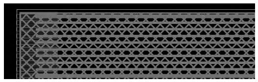
Figure 2 Conventional Mesh Copper Reference Plane Design
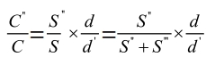
In order to achieve the design goal of C'/C=1 without changing the line width W, the use of a mesh reference plane is inevitable. Thus, there is the FPC (Flexible Printed Circuit) routing capacitance C'' (mesh reference plane):
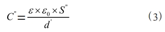
S″ is the projection area of the FPC routing on the mesh reference plane, with the same layer spacing as the solid copper reference plane FPC, and the spacing is also d′. By taking the ratio of equations (1) and (3), we can obtain:
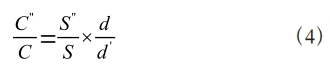
The design goal becomes to achieve C'/C=1. By decomposing and analyzing the mesh, that is:
![]()
Sn is the projection area of a single mesh
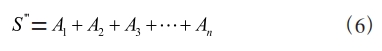
An is the non-projection area of a single mesh;
S″ is the total projection area of the FPC routing on the mesh reference plane, which is the sum of the non-projection areas of the routing;
If C'/C=1, then we get: k=d/d' - 1
From the above analysis, it can be seen that the duty cycle k of the mesh reference plane is related to the layer spacing of the FPC and the normal solid copper FR4. In this paper, the value of d is approximately 4 mil, and the maximum value of d' is 1 mil, with a minimum of 0.4 mil. From this, we can obtain that the range of k values is: [3 → 10]. The above analysis in this paper assumes that the dielectric constants of FPC and FR4 materials are equal, but in reality, there are differences between them, which will result in numerical deviations. The range of k values will shrink and be in decimal form. However, when using a mesh copper reference plane, integers are usually chosen as the selectable values. Therefore, in actual design, according to the description in this paper, the allowable values for the duty cycle k are: 4, 5, 6, 7, and 8, these five integers.


