- Flex PCB Blog
- Reflow Soldering PCB Temperature Curve Explanation
- What is FPC
- Special attention points for flexible circuit wiring
- Multilayer PCB Stack-up Basics | PCB Knowledge
- PCB Protection: Potting or Conformal Coating? | PCB Knowledge
- FPCway: Specialized manufacturer of flexible printed circuit boards and rigid-flexible printed circuits
- Future Trends of Flexible Circuit Boards
- Rigid-Flex PCB Stack-up for Impedance Controlled Designs
- Control Impedance Between Rigid PCB and Flex PCB
- Flex PCB Reliability and Bendability
- Normal Flex PCB Specifications
- Flex PCB Polyimide Coverlay and Solder Mask
- Flex PCB Boards and Connectors
- About RA Copper and ED Copper
- Introduction of Flexible PCB
- 5 Tips For Designing Flexible PCB
- Advantages of FPC (Flexible PCB)
- Evolution of the Flex Printed Circuit Board
- Benefits of Using Flex Circuit Boards
- Why Rigid-Flex PCBs are Economical?
- Flexible PCB vs Rigid PCB
- Development of Flexible printed circuit board (FPC) market
- Traditional Manufacture Engineering of FPC Substrate
- Development Trend of FPC Board
- Flex PCB and the Manufacturing
- About Flex PCB design
- About Flex PCB and Assembly
- How to Ensure Flex PCB Design Success
- How to Select the Appropriate FPC Materials?
- The Differences In Rigid PCB, Flex PCB and Rigid-Flex PCB
- Flex-Rigid PCB Design Guidelines
- Beneficials for Polyimide Flex PCB Boards
- About Stiffener on Flex PCB FPC circuit Boards
- About ENIG and ENEPIG
- PCB Surface Finish Comparison
- Copper Thickness for FPC Boards
- Interconnect Solutions for Flexible Printed Circuits and Etched Foil Heaters
- Advantages and Disadvantages of Rigid-Flex PCB
- About FPC Plating Process
- About EMI shield design for Flex Printed Circuit Board
- PCB Assembly Blog
- FPC Research Blog
Electromagnetic interference (EMI) is associated with every electronic device we use nowadays.
If you turn on your radio set and TV simultaneously, you will experience the noisy disturbance from TV interfering with the radio signal and vice-versa. We can also experience this when we board a plane and are asked to switch off the electronic devices by the crew. This is to avoid interference of mobile and electronic device signals with the plane’s navigational signals. This is the reason why EMI/EMC study and analysis is important. Does your product’s radiation disturb other devices present nearby?
EMI Shielding Design Challenges
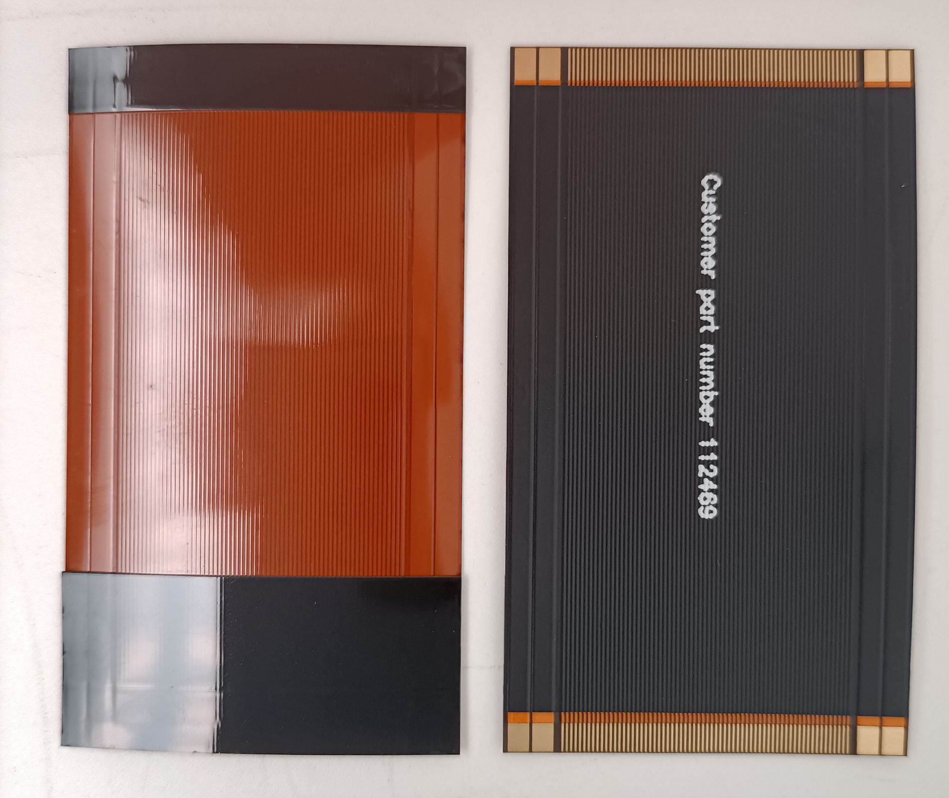
As we all know, the flex circuit EMI shielding added will create multiple design challenges that require careful review to ensure a successful part number.
All EMI shielding will increase both the total flex circuit board thickness and cost. The thickness increased is most often the critical issue. The normal EMI shield thickness is 22um, but we also has 10um thickness EMI shield. It can easily lead to the bending effect get worse. This creates a reliability/mechanical breakage concern. The added cost is also should concern. The Shielding is often combined with other electrical requirements; the most common is controlled impedance. This further increases the flex thickness and compounds the challenge of meeting both the electrical and mechanical design requirements. The flexible circuit industry has multiple solutions that can be applied, which will eliminate both the absorption and/or radiation of interference noise.
What should we pay attention to EMI shield design to avoid the interfering?
1. Keep your signals separate. Keep high speed traces ( clock signals) separate from low speed signals, and analog signals separate from digital signals.
2. Keep return paths short.
3. Route differential traces as close as possible. This increases the coupling factor, bringing influenced noise into the common mode which is less problematic for a differential input stage.
4. Use vias wisely. Vias are necessary because they let you take advantage of multiple layers in your boards when routing. Designers must be aware that they add their own inductance and capacitance effects to the mix, and reflections can occur from a change in characteristic impedance.
5. Avoid using vias in differential traces. If you must, use an oval anti-pad shared by the two vias to reduce parasitic capacitance.
6. Singled sided FPC EMI shield is not working, you need design it as a dual flex pcb at least or double sided or multilayers FPC.
7. Avoid sharp right-angle bends. Capacitance increases in the 45° corner region changing the characteristic impedance and leading to reflections. This can be mitigated by rounding right angles.
8. EMI minimum solder mask opening should be more than 0.8mm, and the solder mask area need to far away from the trace more than 0.2mm.
If you have any Flex PCB boards that need do EMI shield, feel free to contact us by sales@fpcway.com and we will back to you shortly.