- Flex PCB Blog
- PCB Assembly Blog
- FPC Research Blog
- Preparation of FPC based on ultrasonic spraying method_4_Experimental Results
- Preparation of FPC based on ultrasonic spraying method_3_Experimental Procedure
- Preparation of FPC based on ultrasonic spraying method_2_Experimental Platform and Principle
- Preparation of FPC based on ultrasonic spraying method_1_abstract
- Research on Layout Design Method of Ultra-thin FPC_4_Analysis of Layout Design Methods
- Research on Layout Design Method of Ultra-thin FPC_3_Analysis of Layout Design Methods
- Research on Layout Design Method of Ultra-thin FPC_2_Analysis of Layout Design Methods
- Research on Layout Design Method of Ultra-thin FPC_1_introduction
- Research progress on polyimide FPC_2_the field of FPC
- Research progress on polyimide FPC_1_Introduction
- Analysis of Vibration Characteristics of FPCBs _4_Summary
- Analysis of Vibration Characteristics of FPCBs _3_Finite Element Analysis
- Analysis of Vibration Characteristics of FPCBs _2_Theory of Vibration Analysis
- Analysis of Vibration Characteristics of FPCBs Under Random Vibration_1_Introduction
- Design Methods for FPCBs_5_Practical Application
- Design Methods for FPCBs_4_Electrical Circuit Design and Examples
- Design Methods for FPCBs_3_Structure Design Method and Examples
- Design Methods for FPCBs_2_Component Selection Methodology and Examples.
- Research on Design Methods for FPCBs
- Application of MPW technique for FPCBs _4_Summary
- Application of MPW technique for FPCBs_3_Experimental results
- Application of MPW technique for FPCBs_2_Experimental setup
- Application of MPW technique for FPCBs_1_Principle of MPW
- Application of FPCB in PC motherboards_4_ Results and discussion
- Application of FPCB in PC motherboards_3_ Numerical analysis
- Application of FPCB in PC_2_ Experimentation
- Application of FPCB in PC motherboards
- A Bus Planning Algorithm for FPC Design _4_Experimental result
- A Bus Planning Algorithm for FPC Design _3_Proposed Algorithm
- A Bus Planning Algorithm for FPC Design _2_Preliminaries
- A Bus Planning Algorithm for FPC Design _1_Introduction
A Bus Planning Algorithm for
FPC Design in Complex Scenarios_2_Preliminaries
II. Preliminaries
1. Terminologies
An industrial complex FPC board is shown in Fig.2, the pin area is distributed around the central area, and different areas are connected through channels. Mean- while, the connection between different areas is similar to bus routing, and engineers also refer to this feature when routing.
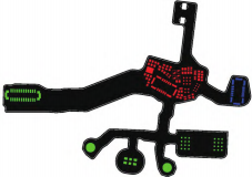
Fig. 2. An industrial FPC board.
According to the characteristics of FPC, the PAI model shown in Fig.3 can be obtained by using a hier- archical clustering algorithm and some geometric pro- cessing. PAI ensures that most pins are concentrated in a certain number of areas, and there are no or only a few pins in the channel. The pin area is further divided into the side pin area (SPA) and center pin area (CPA); the number of CPA might be zero in some in- dustrial complex FPC. ![]() is the channel,
is the channel, ![]() is the bus that
is the bus that ![]() to
to ![]() ,
, is the single net that belongs to CPA, L is the layer, BL is the boundary line between pin areas and the channel. For SPA, there is one and only one boundary line.
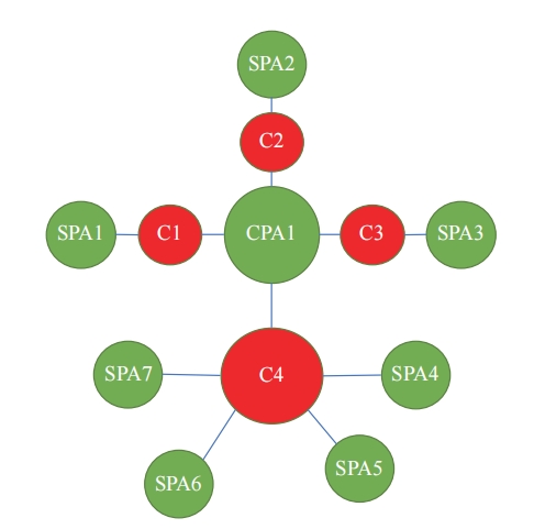
Fig.3.PAI model,wihch is an undirected graph.
2. Problem Formulation
FPC is suitable for divide and conquer from the PAI model. The whole board routing problem can be divided into the pin area internal rout- ing subproblem and the channel routing subproblem. The routing flow of a single net is transformed into starting pin to CP and CP to the ending pin. The CPs are on the area boundary, and the resource distribution within the pin area and the channel is reflected in the location selection of the CPs. Finally, the complex FPC bus planning problem can be described as follows: Given a board, divide it into some SPAs and CPAs, consider resource distribution and routability by optimizing the selection of CP location, output the 3D coordinate of the CPs, which are on the corresponding BL. The X and Y coordinate are the locations of CP in the cur- rent layer while Z axis is the layer. Net in each region only corresponds to one CP. The PAI model is a representative model in FPC. The observation of several actual industrial FPC boards conforms to the description of this model.


