- Flex PCB Blog
- PCB Assembly Blog
- FPC Research Blog
- Preparation of FPC based on ultrasonic spraying method_4_Experimental Results
- Preparation of FPC based on ultrasonic spraying method_3_Experimental Procedure
- Preparation of FPC based on ultrasonic spraying method_2_Experimental Platform and Principle
- Preparation of FPC based on ultrasonic spraying method_1_abstract
- Research on Layout Design Method of Ultra-thin FPC_4_Analysis of Layout Design Methods
- Research on Layout Design Method of Ultra-thin FPC_3_Analysis of Layout Design Methods
- Research on Layout Design Method of Ultra-thin FPC_2_Analysis of Layout Design Methods
- Research on Layout Design Method of Ultra-thin FPC_1_introduction
- Research progress on polyimide FPC_2_the field of FPC
- Research progress on polyimide FPC_1_Introduction
- Analysis of Vibration Characteristics of FPCBs _4_Summary
- Analysis of Vibration Characteristics of FPCBs _3_Finite Element Analysis
- Analysis of Vibration Characteristics of FPCBs _2_Theory of Vibration Analysis
- Analysis of Vibration Characteristics of FPCBs Under Random Vibration_1_Introduction
- Design Methods for FPCBs_5_Practical Application
- Design Methods for FPCBs_4_Electrical Circuit Design and Examples
- Design Methods for FPCBs_3_Structure Design Method and Examples
- Design Methods for FPCBs_2_Component Selection Methodology and Examples.
- Research on Design Methods for FPCBs
- Application of MPW technique for FPCBs _4_Summary
- Application of MPW technique for FPCBs_3_Experimental results
- Application of MPW technique for FPCBs_2_Experimental setup
- Application of MPW technique for FPCBs_1_Principle of MPW
- Application of FPCB in PC motherboards_4_ Results and discussion
- Application of FPCB in PC motherboards_3_ Numerical analysis
- Application of FPCB in PC_2_ Experimentation
- Application of FPCB in PC motherboards
- A Bus Planning Algorithm for FPC Design _4_Experimental result
- A Bus Planning Algorithm for FPC Design _3_Proposed Algorithm
- A Bus Planning Algorithm for FPC Design _2_Preliminaries
- A Bus Planning Algorithm for FPC Design _1_Introduction
A Bus Planning Algorithm for
FPC Design in Complex Scenarios_3_Proposed Algorithm
In this section, we introduce the specific optimiza- tion algorithm of the CP location problem. First, we give an overview of the whole process and then intro- duce the proposed algorithm in detail.
Fig.4 is the overall flow of the proposed algorithm, which can be divided into two parts: (1) Build the whole board bus topologically non-crossing sequence; (2) CP iterative optimization.
1. Bus topologically non-crossing sequence
Traditional DPS requires routing iteration to get the best sequence expansion. This paper only uses the idea of erasing the same symbol of the sequence after expansion to judge that the topology does not cross; that is, after expanding into a circular sequence, as shown in Fig.5(a), the bus B and A expand into a circu- lar sequence BAAB, we can observe that symbol A is repeated due to the concatenation, it means that net A can be connected without crossing. If a sequence can- not be completely erased, as shown in Fig.5(b), it is proved that the bus still in the sequence cannot be on the same layer.
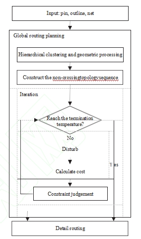
Fig.4. The flow of the proposed algorithm
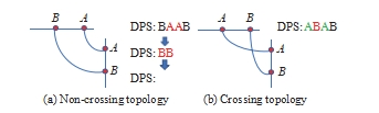
Fig.5.using DPS to judge whether there is a crossing.
The channel area of FPC cannot be detoured or punched when routing due to the direct guidance of the outline and the limitation of materials, so the topologic- al non-crossing must correspond to the non-crossing paths of the actual routing. Besides, based on the PAI model, we can first deal with the connection between buses and then handle the single net in the bus. Fig.6(a) shows the topological connection based on PAI; it can be seen that the connection relationship of FPC buses has many topological crossings. In this step, the specific location of the CPA in the DPS sequence can- not be determined due to the net can detour in the CPA. Therefore, the processing of the CPA is turned to the disturbance, and we only considered the non-cross- ing topological of SPA in this step. Fig.6(b) shows the connection relationship after shielding the CPA, and the sequence expanded in clock sequence is shown in Fig.7(a). This sequence is finally mapped to the bound- ary line of each SPA as shown in Fig.7(b). This order will not be changed after it is determined, which means that as long as the boundary satisfies this order rela- tionship, there will be no topological cross between buses, and it will be used as a constraint for the sub- sequent iteration process. The single net in CPA con- nected with SPA is randomly inserted between bus se- quences during the subsequent disturbance.
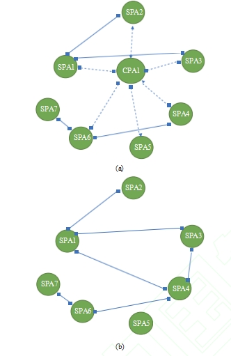
Fig.6
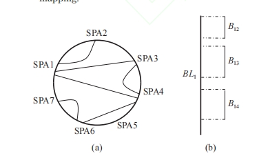
Fig.7
2. CP iterative optimization
In this section, we introduce the cost system and disturbance strategy of iteration in detail. We use simulated annealing (SA) to comprehensively consider the costs and constraints of SPA and channel. SPA and channel have different characteristics, so the two regions need to be considered separately to achieve better results.
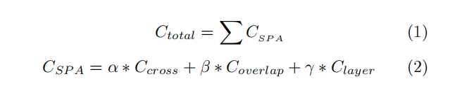
where ![]() is the cost of SPA,
is the cost of SPA, ![]() is the cross cost of the SPA,
is the cross cost of the SPA,![]() is the overlapping cost of the fly- line and obstacle in SPA,
is the overlapping cost of the fly- line and obstacle in SPA,  is the exchange layer cost. The goal is to minimize the total cost
 ![]() .
. ![]() , are custom parameters and the values used in the experiment are 100、1、10, respectively. This is be- cause the unit
, are custom parameters and the values used in the experiment are 100、1、10, respectively. This is be- cause the unit ![]() is length, and thus we convert other units into length units. The selected key parameters of SA are listed in Table 1.
is length, and thus we convert other units into length units. The selected key parameters of SA are listed in Table 1.
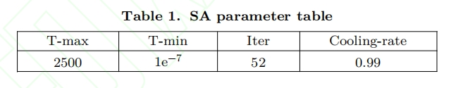
T-max is the start temperature, T-min is the ter- mination temperature, Iter is the Markov chain length.
1) Fly-line crossing cost
The fly-line crossing has certain representative sig- nificance in the SPA, if the fly-line crosses, it means that a detour is necessary to solve the problem. Mul- tiple fly-line crosses at the same time may lead to the inability to connect the net no matter how it is detour. As such, the cross cost is considered, which can be given as:
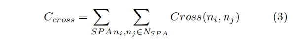
where Cross(ni , nj ) represents the crossing of net ni and nj in SPA. NSPA is the total net in SPA.
2) Overlapping cost
Considering both the SPA and the CPA, there always exist various obstacles, such as components and forbidden routing areas, and the netlist must bypass these obstacles, which bring additional length. It is realistic to measure the manual routing, which can be expressed as
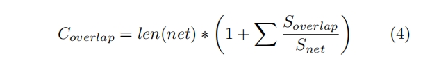
where len(net) is the length of the fly-line, Soverlap is the area where the obstacle overlaps the rectangle with this fly-line as the diagonal, Snet is the area of this rect- angle, which is shown in Fig.8.
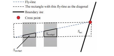
Fig.8
3) Exchange layer cost
It is often difficult for topology strategy to estimate the real punching information; however, considering a single net, its optimal punching quantity can be determined. Especially, if the starting pin and ending pin of a net are located on the same layer, it is better not to change the layer; otherwise, it is encouraged to use only one via if the type of via allows. In this way, one can simplify counting the number of vias:
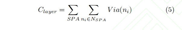
where Via(ni ) indicates the cumulative number of holes punched in the net ni , this value can be obtained by counting the number of changes in the layer of the CP to which the net ni belongs in the PAI model.
4) Non-crossing constraint in the channel
Bus non-crossing constraint only ensures that thereis no cross between different SPAs; otherwise it would cause serious cross overs when the net from CPA is inserted into the bus sequence randomly. We know the layer assignment of CP after disturbance, so it is promising to judge the topology cross of each layer of each channel. For example, as shown in Fig.9, BL1is the boundary line of SPA1 , B12 , B13 and B14 are the relative order of bus mapping on the boundary line after non-crossing topology expanded. A single net from CPA is randomly inserted into the interval between buses during the disturbance, then perform sequence cross judgment again. If there is the cross in the channel the random results will be passed.
3. Random disturbance strategy
Both the fly-line crossing cost and obstacle overlapping cost are dependent on the location of CPs, and it is often inconvenient to directly disturb the coordinate of the CPs. As such, we choose to change the location of the point indirectly by disturbing the width of the net to achieve the purpose of disturbing the location of the CPs. The minimum distance constraint between nets shall be strictly guaranteed. The net connect to the CPA will be randomly inserted into the bus interval on the corresponding boundary at each iteration; this is be- cause in the previous step B only the net from the SPA is considered, and the net from the CPA cannot join the circular sequence formed by the SPA. The net in the bus will also change layers or change the order in sequence randomly.


