- Quick FPC Prototype
- Flex PCB Production
- Flex PCB Production | FPCway
- Rigid-Flex PCB Prototype
- Flex PCB Assembly
- Rigid-Flex PCB Assembly
- Rigid PCB and Assembly
- Electronic PCBA Design
- Components Sourcing
- SMD Stencil
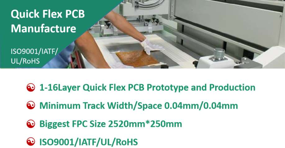
We are specialized in the quick FPC prototype for 1-16L flex PCB boards and also could do flexible circuit PCB board production in affordable price, high quality and quick lead time. Working in Flexible PCB board industry for 10+ years, we now have a 5,000sqm Flex PCB factory, the monthly flex PCB production capacity are more than 15,000sqm. And we have a team of more than 200 staffs, and more than 20 senior executives have more than ten years of experience in Flex PCB industry. With these experiences and continue to update the equipment, we maintained the advanced technical capability and high FPC prototype and FPC production capacity in the Flex PCB industry.
FPCway is a flex circuit board manufacturer that provides fast flex PCB prototypes, short-runs, and production. We offer flex PCB material and components to build high-quality flexible printed circuit boards.
And our FlexIible PCB circuit boards now are highly used in computer, communication network equipment, mobile phone, digital camera, instrumentation, aerospace instrument, biomedical, home appliance and lighting, drone, smart wear, smart home, bluetooth, car, industrial control, robot, tablet, LCD, projection Instrument, car navigation, security and other high-tech fields, etc.
Lead Time for Flex PCB | ||||
| Layer | Standard FPC Specification | Quickest Protype | Standard Prototype | Production Time |
1L | 1Layer, PI, 0.05mm-0.2mm thickness, 6um-100um base copper, Yellow Coverlay, White silkscreen, ENIG | 1-2 Days | 5-7 Days | 8-10 Days |
2L | 2Layer, PI, 0.08mm-0.3mm thickness, 6um-100um base copper, Yellow Coverlay, White silkscreen, ENIG | 1-2 Days | 5-7 Days | 8-10 Days |
4L | 4Layer, PI, 0.2mm-0.4mm thickness, 6um-100um base copper, Yellow Coverlay, White silkscreen, ENIG | 3-4 Days | 8-10 Days | 10-12 Days |
6L-16L | Up to the customers requirements. | 6-8 Days | 12-14 Days | 14-18 Days |
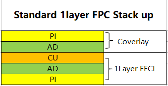
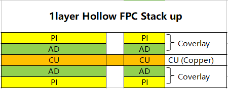
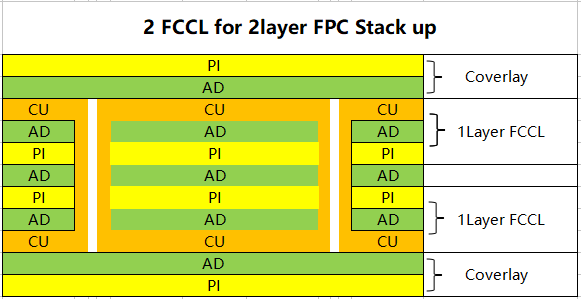
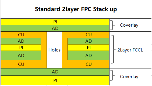
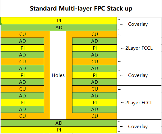
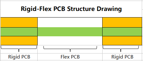
FPC has single sided flexible PCB board, double sided flex circuit PCB, multi-layer Flex PCB and Rigid-flex PCB circuit board. The flex PCB material is polymide FCCL and it has high heat resistance and stable size. Following are the common layer structure and stack up for Flex circuit PCB for your reference. The FPC final thickness could be adjusted flexibly with different thicknesses of PI, adhesive, copper, etc.
| FCCL Material Thickness | ||||
| Coverlay/Solder Mask | 2Layer FCCL | |||
| PI (12.5/25/50/100um, etc.) | Copper (6/9/12/18/35/70/100um, etc.) | |||
| AD (15/25/35/50um, etc.) | AD (0/12.5/20/25um, etc.) | |||
| PI (12.5/25/50/100um, etc.) | ||||
| 1Layer FCCL | AD (0/12.5/20/25um, etc.) | |||
| Copper (6/9/12/18/35/70/100um, etc.) | Copper (6/9/12/18/35/70/100um, etc.) | |||
| AD (0/12.5/20/25um, etc.) | ||||
| PI (12.5/25/50/100um, etc.) | ||||
| Flex PCB Stack-up Structure | |
 |  |
 |  |
 |  |
Flex PCB Technical Capabilities | |||
FPC Layer | |||
| NO. | ITEM | Standard Capabilities | Special Capabilities |
| 1 | FPC Layer | 1-12L | 1-16L |
FPC Material | |||
| 2 | Base Material | PI (12.5um, 25um, 50um) | 100um |
| 3 | Copper Type | RA Copper: 12um, 18um, 35um, 70um ED Copper: 12um, 18um, 35um, 70um | 6um, 9um, 100um |
| 4 | PI Coverlay | 12.5um, 25um, 50um | 100um |
| 5 | Adhesive | PSA Adhesive: 50um-100um (3M467, Tesa 8853, Tesa 8854, etc.) | |
| 6 | Hot-Press Adhesive: 13um, 25um | ||
| 7 | Stiffeners | PI Stiffener: 12.5/25/50/75/100/125/150/200/250 (um) | |
| PET Stiffener: 0.125/0.188/0.25(mm) | |||
| FR4 Stiffener: 0.1mm-1.6mm | 2mm | ||
| SUS Stiffener: 0.1mm-0.5mm | |||
| Aluminum Stiffener: 0.1mm-0.5mm | |||
| 8 | EMI shielding film | HCF-6000G, PC800, etc. | 100um |
Board Size & Thickness | |||
| 9 | Biggest Board Size | 500mm*600mm | |
| 10 | Longest Board Size | 250mm*2520mm | |
| 11 | Biggest Board Thickness | 2.0mm | |
| 12 | Thinnest Board Thickness | 0.05mm | |
| 13 | Thickness Tolerance | 0.05mm~0.24mm: ±0.03mm 0.25mm~0.47mm: ±0.05mm | |
Drill | |||
| 14 | Minimum Hole Size | 0.1 mm | 0.025mm |
| 15 | Holes Size Tolerance | ±0.05 mm | |
| 16 | Holes Posistion Tolerance | ±0.05 mm | |
| 17 | Minimum vias Pad Size | 0.3mm | 0.2mm |
| 18 | Minimum Annular Ring Size | 0.1mm | 0.075mm |
| 19 | Blind/Buried Vias | Yes | |
Copper Tracks and Plating | |||
| 20 | Minimum Track Width/Space (35um Copper) | 0.1mm/0.1mm | |
| 21 | Minimum Track Width/Space (18um Copper) | 0.07mm/0.07mm | 0.05mm/0.05mm |
| 22 | Minimum Track Width/Space (12um Copper) | 0.04mm/0.04mm | 0.035mm/0.035mm |
| 23 | Track Width Tolerance | 20% | 0.02mm |
| 24 | Tracks/Pads Position Tolerance | ≥0.06 mm | ≥0.05 mm |
| 25 | Tracks/Pads To Board Edge | ≥0.15 mm | ≥0.05 mm |
| 26 | Golden Finger Pitch Tolerance | Pitch:10~20mm : ± 0.03mm, Pitch:20~50mm : ± 0.05mm | |
| 27 | Copper Plating Thickness | 8-20um | |
| 28 | Hole Copper Thickness | 8-20um | 35um |
| 29 | Minimum Copper Thickness for Hollow Out FPC | 35um | |
Surface Finish | |||
| 30 | ENIG | AU: 1-2u" Thickness NI: 40-120u" Thickness | 3u” Thickness |
| 31 | Electrolytic Nickel Gold (Hard Gold Plating) | AU: 1-50u” Thickness NI: 80-320u" Thickness | |
| 32 | Immersion Silver | Ag: 6-12u" Thickness | |
| 33 | OSP | 8-16u" Thickness | |
| 34 | Immersion Tin | SN: 10-60u" Thickness | |
| 35 | Tin Plating | SN: 5-30um Thickness | |
| 36 | ENEPIG | Au:1-4u" Thickness NI: 120-200u" Thickness Pd:1-6u" Thickness | |
Coverlay | |||
| 37 | Coverlay Opening Size Tolerance | ±0.1 mm | ±0.03 mm |
| 38 | Minimum Drilling Size on Coverlay Opening | 0.45mm | 0.2mm |
| 39 | Minimum Square Size on Coverlay Opening | 0.7mm*0.7mm | 0.2mm*0.2mm |
| 40 | Coverlay Opening Position Tolerance | ±0.1 mm | ±0.03 mm |
| 41 | Coverlay Align Tolerance | ±0.1 mm | ±0.02 mm |
| 42 | Excessive Glue | ≤0.15 mm | |
| 43 | Minimum Area of Excessive Glue | ≤20% Pads Area | |
Solder Mask and Silkscreen | |||
| 44 | Solder Mask Thickness | 15um +/-5um | |
| 45 | Solder Mask Tolerance For Opening Size | +/-0.05mm | +/-0.02mm |
| 46 | Solder Mask Tolerance For Opening Position | 0.1mm | +/-0.02mm |
| 47 | Minimum Silkscreen line width | 0.13mm | |
| 48 | Minimum Silkscreen Gap | 0.2mm | |
| 49 | Minimum Silkscreen Position Tolerance | +/-0.3mm | |
| 50 | Minimum Silkscreen height | 0.8mm | |
| 51 | Minimum Solder Mask Bridge | 0.13mm | |
Board Outline & Stiffeners | |||
| 52 | Board Outline Tolerance with Steel Die | ±0.1 mm | ±0.03mm |
| 53 | Board Outline Tolerance with Knife Die | ±0.2 mm | |
| 54 | Minimum Gap Between Drilling and Board Edge | ≥0.5 mm | |
| 55 | PSA Position Tolerance | ±0.2 mm | |
| 56 | Stiffeners Position Tolerance | ±0.2 mm | |
FPC E-Test | |||
| 57 | Test Voltage | 10-50V | |
| 58 | Insulation Test Impedance | ≥10MΩ | |
| 59 | Conduction Test Impedance | ≤50Ω | |
| 60 | Impedance Tolerance | 10% | |
FPC Physical Property | |||
| 61 | Solderability Test | 245±5℃, 3 Seconds For One Time, Soldering Area≥95% | |
| 62 | Thermal Shock Test | 288±5℃, 10 Seconds Per 3 Times, No Delamination and No Bubbles | |
| 63 | FCCL Peel Strength | ≥0.8kgf/㎠ (1cm width sample) | |
| 64 | Coverlay Peel Strength | ≥0.8kgf/㎠ (1cm width sample) | |
| 65 | Stiffeners Peel Strength | 0.15 N/mm (Hot-Press Adhesive) 0.49 N/mm (PSA Adhesive) | |
